
Photovoltaic (PV) cells are also known as Solar cells. A group of solar cells forms a solar photovoltaic panel or solar photovoltaic module. Together with the downstream devices from solar wiring, circuit breaker, solar charger, battery, solar inverter all form a Photovoltaic System.
They are magical technology that convert the sunlight into electricity to store or power other devices including artificial lights. So whats wonderful about them ? How it works ? How it is made ? Lets find out.
Photovoltaic
“Photo” means lights, or photons or electromagnetic waves in the spectrum of persivable light. “Volt” means electrical potential diffrence, which cause the flow of electrons and generate current – electricity.
Photovoltaic means materials that can exhibit movement of electron when been hit by a light source (natural or artificial source with sufficient wavelength and energy).
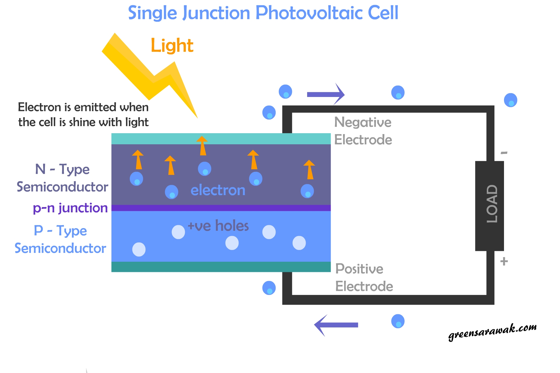
The operation of a photovoltaic (PV) cell requires three basic attributes:
- The absorption of light, generating either electron-hole pairs or excitons.
- The separation of charge carriers of opposite types.
- The separate extraction of those carriers to an external circuit that complete the circulation of electrons.
In Photovoltaic Cells there two distinctive different group, namely single junction and multi junction cells.
Single junction solar cells have just one p-n (Positive-Negative) junction, while multi junction solar cells have more than one p-n junction. p-n junction are boundary between two semiconductor materials, where one of it is electron rich semiconductor (N-type) while the other one is electron depleted (P-type).
Single Junction and Multi Junction Photovoltaic Cell
Single junction Photovoltaic cells are found in most conventional solar cells available in the market. Crystalline Silicon solar cell (mono and poly) is one of the great example.
The pure silicon that is doped (add with trace amount of impurity) with Boron will form the P-Type semiconductor while the pure silicon that is doped with Phosphorus will form the N-Type Semiconductor.
When the photons in the sunlight hit the solar cell and removes an electron from the n-region (with high electron concentration), the dislodged electron escapes from this region, and through a circuit, reaches the p-region (low electron concentration). This flow of electrons constitutes the electricity.
The highest theoretical efficiency possible with a single junction solar cells is about 34% (Shockley Queisser Efficiency Limit). More information about the efficiency is at the next few chapter.

In quest for higher efficiency photovoltaics, multiple layer of p-n junction is created by stacking multiple layer of different p-type and n-type semiconductor. This allow a wider spectrum of light energy being able to be converted into electricity.
Different semiconductor material such as Gallium indium phosphide (GaInP), gallium indium arsenide (GaInAs), and germanium (Ge) are used. Each of these semiconductors uses a different wavelength range of sunlight to generate electricity.
Types of Solar Cell
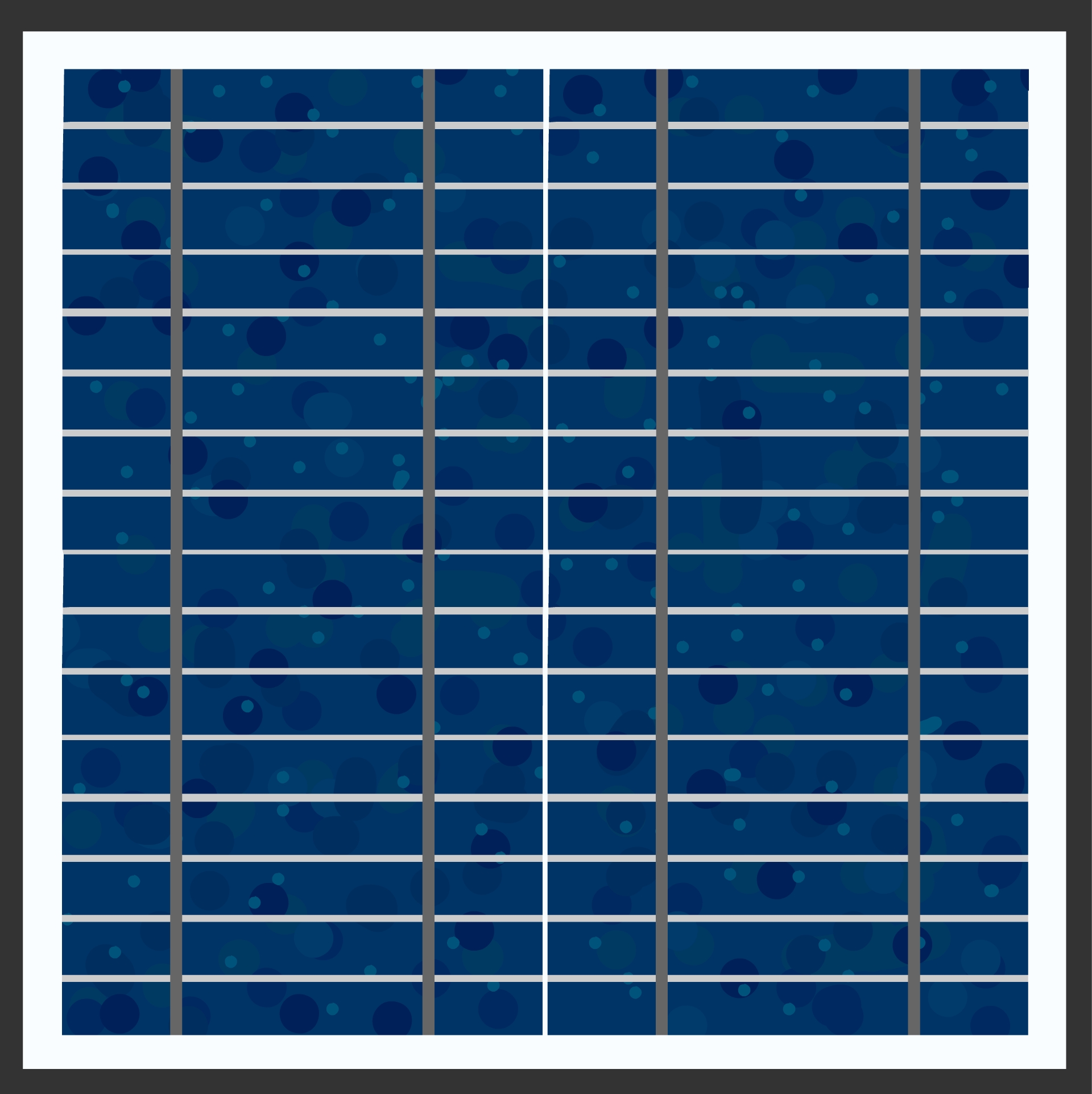
The most common is the Crystalline Silicon (c-Si) type. As the name indicated, it is made from silicon crystals. It occupy nearly 90% of the current solar usage in the market. however there is many type of solar panel out in the market. It is all differ by its build material and forms.
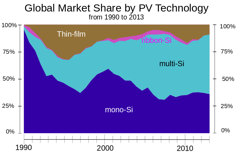
Source: Fraunhofer ISE, Report, current edition. data from archived edition, July 28, 2014, page 18. Public Domain Image @ wikimedia
First we look at the two most common Silicon Solar Photovoltaics – Monocrystalline and Polycrystaline Photovoltaics.
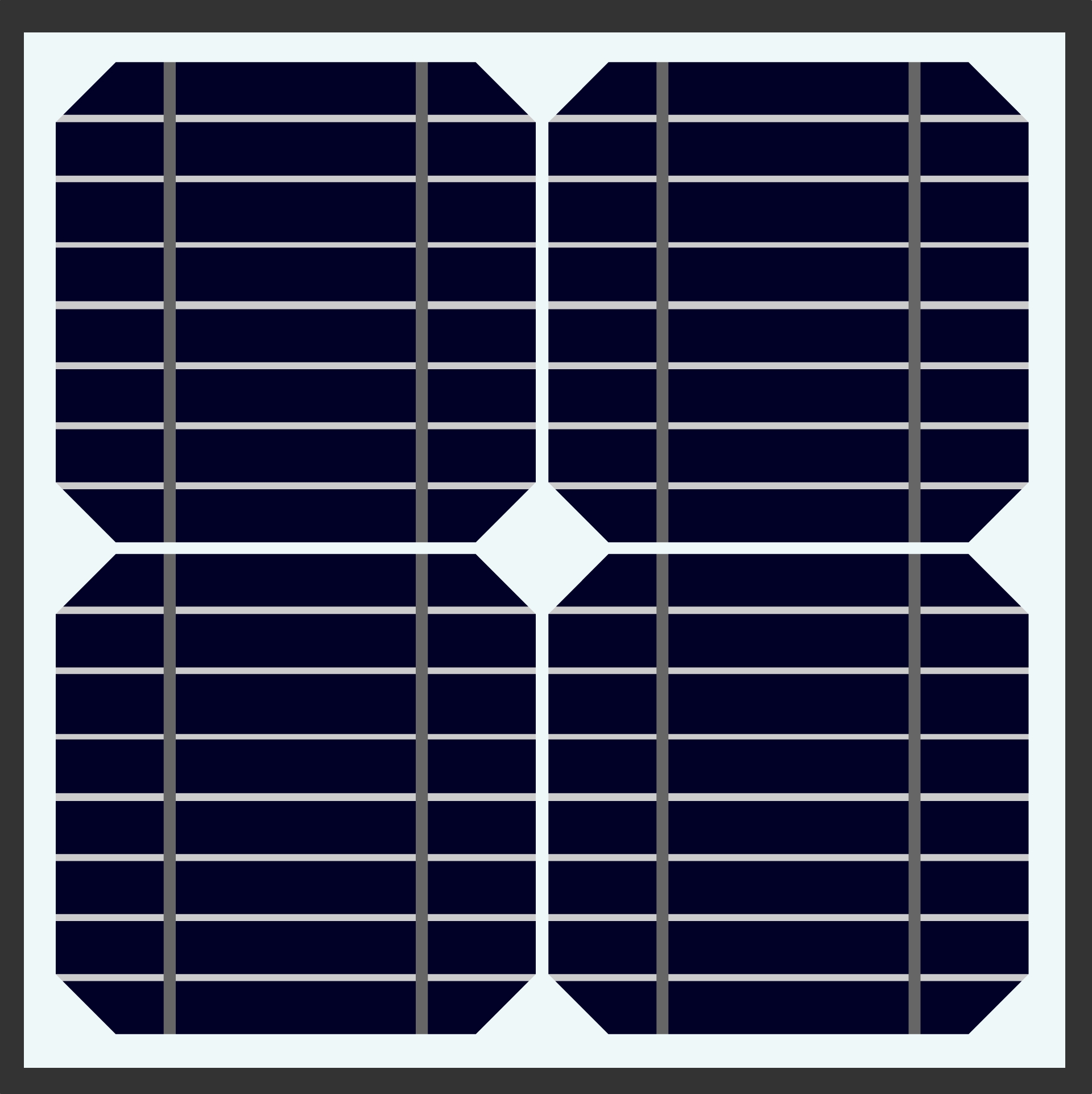
Mono-Crystalline Silicon Solar PV (Monocrystaline Solar Cells) – The most efficient Silicon based solar cells, which is made from wafer from a artificially grown single silicon crystal via Czochralski process. It have the highest purity, appears dark and uniform and usually have a distinct feature of cut edges as four sides are cut off from a crystal ingot (cylyndrical in nature) to form a uniform wafer. It performs better in warm temperature and low light, with efficiency ranging 15-22%. It is also more expensive that polycrystaline solar cells.
Poly-Crystalline Silicon Solar PV (Polycrystaline Solar Cells) – The most economical Silicon based solar cells. It is known as polysilicon (p-Si) and multi-crystalline silicon (mc-Si). The distinct patchy feature is due to multiple interlocking silicon crystals that a grown together. Czochralski process is not used, instead the molten silicon is poured into a square mold to form the crystal. Hence it is less purity and cheaper to produce. Slightly less efficient than monocrystaline, expecially in higher heat, and have efficiency of 13-18%. To make up for the slightly less efficiency, poly solar will have larger areas than mono for panels compared with same wattage. Moreover newer poly panels had efficiency that can compete with mono panels.
Next we look at other variance of solar cells in the market – Thin Film Solar Cells.

Thin-Film Solar Cells (TFSC) – Instead of using classical silicon crystals (crystals are thick, hard but brittle and will crack under bending pressure), photovoltaic materials is deposited very thinly on a backing substrate, making it more light and flexible. Thin-film panels simple to manufacture, appear homogeneous and looks appealing, and flexible. Efficiency variable depends on photovoltaic materials. Thin-film panels can be constructed from a variety of materials, with the main options being amorphous silicon (a-Si), the most prevalent type, cadmium telluride (CdTe) and copper indium gallium selenide (CIS/CIGS).
- Amorphous Silicon (a-Si) Solar Cells – Instead of Silicon crystals, Silicon is deposited very thinly (very little ammount of silicon – around 1%) on a backing substrate (e.g glass and plastics) . However it is less efficient at around 7% – 9% (best reserarch cell efficiency 13.4%). It can be found in small consumer electronics like the solar powered calculator.
- Cadmium Telluride (CdTe) Solar Cells – a cheaper alternative. It had surpassed the cost-efficiency of crystalline silicon solar panels. The efficiency of solar panels based on cadmium telluride usually operates in the range 9-11% (best reserarch cell efficiency 19.0%). However due to its cost-efficiency, It is being used in multi-kilowatt systems, if land area is not an issue. It occupy 43% of the thin film market shares. Anyway, Cadmium is highly toxic.
- Copper Indium Gallium Selenide (CIS/CIGS) Solar Cells – It can use substrate like glass or other flexible substrate. The efficiency rates for CIGS solar panels typically operate in the range 10-12 % (best reserarch cell efficiency 20.4%). It have the highest efficency of the thin films categrory but it is most expensive of the three.
Building-Integrated Photovoltaics (BIPV) is another upcoming solar technology. It is more like a hybrid or intergration (either crystaline silicon or thin film or both) of solar technology into parts of a building instead of a stand alone solar panel. Facades, roofs, windows, walls and many other things which have contact with sunlight can be combined with photovoltaic material. They are like power generating ninjas, not totally stealthy but more appealing than traditional approach.
How a solar cell is made ?
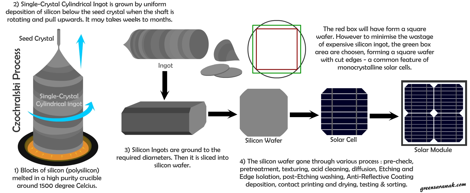
Wondering how the solar cells are made ? It is a complex and yet wonderful concept. We take an example of how to make a Monocrystalline Solar Cell. Althought silicon is abdundant on earth (most common element in the universe), and sand is mainly silicon, but obviously you can’t make solar at home. It all back to how to artificially grow a crystal via Czochralski Process.
Czochralski process is a method of crystal growth used to obtain single crystals (semiconductors, metals and gemstones). High purity polysilicon (only a few parts per million of impurities – formed after reduction and purification of silicon dioxide quartz) is melted in a high purity vacumme crucible around 1500 degrees Celsius.
During this time dopant impurity can be added to the molten silicon to dope (modify its electrical properties of the material) the silicon. A common dopant for n-type silicon (electron concentration more than hole concentration) is Phosphorus. A common dopant for p-type silicon (hole concentration more than electron concentration) is Boron.
A pure silicon rod at the end of a shaft act as a seed crystal will be dipped into the molten silicon and slowly pull up while rotating anticlockwise. The silicon crystal will slowly grow on the seed via uniform deposition of silicon, forming a large cylindrical crystal (or called Boule or Silicon Ingot) below which may weight 200-700kg. The rate of pull, rotation and cooling (temperature gradient) will determine the quality and the size of the crystal formed. This process can takes weeks to months, and accounts for one third of the cost of the monocrystalline solar cell production.
The silicon ingot is later been ground to a specific diameter and sliced with a diamond saw into specific configuration. 125 mm by 125 mm wafers produced from ingots that are approximately 150 mm in diameter, and 156 mm by 156 mm wafers produced from ingots that are approximately 200 mm in diameter. The odd shape of Monocrystaline solar cells with cut edges is mainly because the maximum usable squared surface is determined from a circle to minimize excessive silicon loss.
Later the silicon ingot is sliced to form silicon wafer by wire saw. It is called wafering. It gone through various process to make a solar cell from a wafer.
- precheck and pretreatment :- to select good wafer with specified geometric shape and thickness conformity.
- Texturing :- Random pyramid texture is etched on the surface to reduce reflective loss of incident light.
- Acid cleaning :- to remove post texturing particle remains from the surface.
- Diffusion :- adding dopant to the silicon wafer to make it electrically conductive. For example a pre-doped p-type boron wafer is given a negative (n-type) surface by diffusing them with a phosphorous source at high temperature, creating the positive-negative (p-n) junction.
- Etching & Edge Isolation :- to remove undesired electrical path formed by n-type phosphorus diffuses around wafer edge and the back.
- Post-Etching washing :- remove all particle residues from the etching.
- Anti-Reflective coating deposition :- to reduce surface reflection and increase amount of light absorbed.
- Contact printing and Drying :- Metal inlines are printed on both side of the wafer to create ohmic contacts. Sintering furnance is used to solidify the dry metal paste on the wafer. After drying the wafer can be called solar cells.
- Testing & Cell sorting :- The solar cells is tested under simulation lights and sorted out according to efficiency and grades.
In a polycrytalline solar cell manufacturing, it also underwent the similiar process above, but without Czochralski Process. The high purity polisilicon is crushed and melted, directly cast into square multicrystalline ingots. Without Czochralski Process, the process is much faster and cuts down 20-30% of the cost comparing polycrystalline and monocrystalline.
The Photovoltaic Growth
The United States is the inventor and pioneers of modern solar photovoltaics. It had being the major lead in 1954-1996. American engineer Russell Ohl at Bell Labs patented the first modern solar cell in 1946. The first practical crystalline silicon cell was developed in 1954. Since then the cell efficiency was improved.
Subsequently Japan took the lead as the world’s largest producer of PV electricity in 1997-2004.
Germany took the lead in 2005-2014. The introduction of the Renewable Energy Act in 2000 making renewable energy being piriotise on the grid. Many had invest in the renewable technology causing raise in PV instalations. In 2016 Germany’s installed PV capacity was over the 40 GW mark.
China start to involve in the PV solar industry in the early 2010. China surpassed Germany’s capacity by the end of 2015, becoming the world’s largest producer of photovoltaic power until today and continue growing.
Due to global demand of Photovoltaic increase, maturing of silicon wafer manufacturing, and increasing in number of silicon wafer production plants, the Photovoltaic is become more and more consumer affordable.
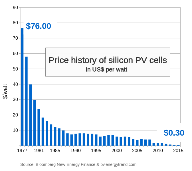
Source: Bloomberg, New Energy Finance & EnergyTrend.com , Public Domain Image @ wikimedia
The myth behind solar efficiency
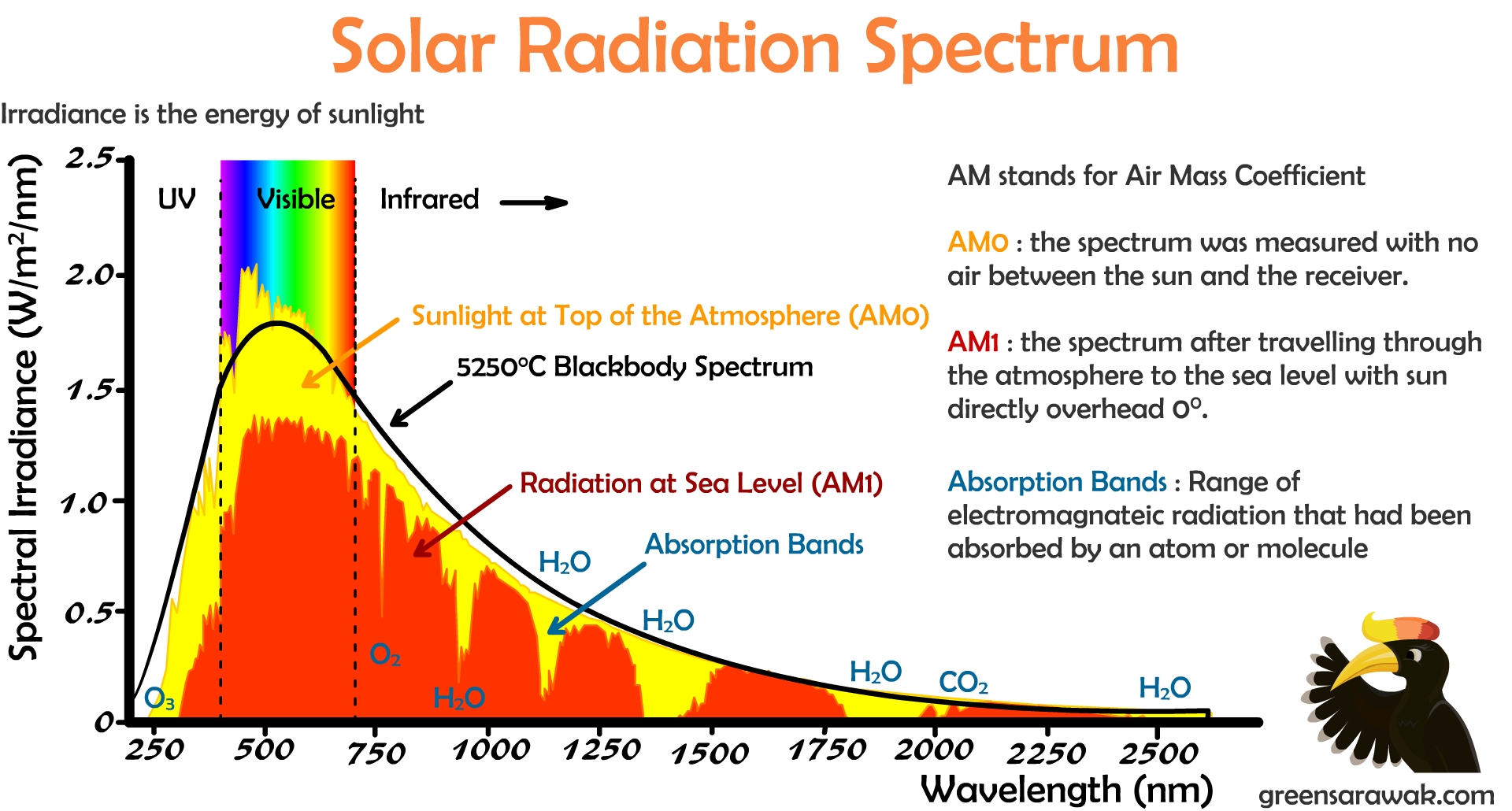
The Earth receives 174 petawatts (PW) of incoming solar radiation at the upper atmosphere. Approximately 30% is reflected back to space while the rest is absorbed by molecules in the atmosphere such as Ozone, Oxygen, and Water, before the sun light reach the sea level.
Solar efficiency basically tells how much rate of the energy of the light been captured and converted to electricity in a square meter.
However there is a limitation of how much photon that a photovoltaic semiconductor material can actually absorbed and turn into electrical energy. Photons which have lower energy (longer wavelength) will not be absorbed. Only photons with energy higher than the bandgap energy can knock off the electrons by creating electron-hole pair in a photovoltaic material and generate electricity, however excess energy from the photon will be converted to heat.
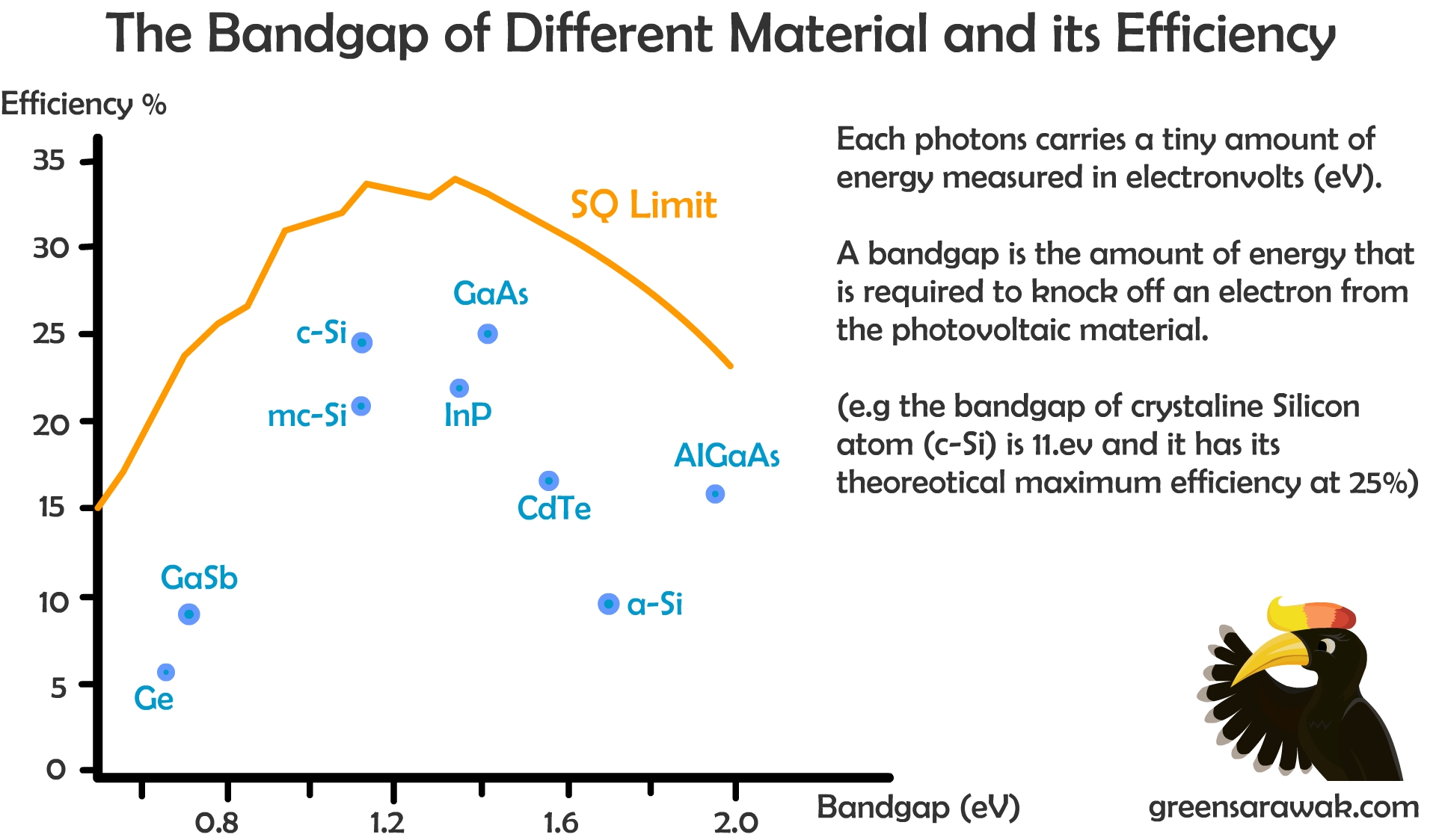
This put to a theoretical maximum efficiency limit of a solar cell with a single p-n junction is able to collect. It is known as Shockley Queisser Efficiency Limit or SQ Limit. The limit places maximum solar conversion efficiency around 33.7% assuming a single p-n junction with a band gap of 1.34 eV (using an AM 1.5 solar spectrum).
AM 1.5 solar spectrum is commonly used as major solar installations and industry lie in temperate latitudes (Europe, China, Japan, the United States of America, northern India, southern Africa and Australia.)
To increase the efficiency of a solar cell beyond the SQ Limit, usually multiple junction solar cells is needed. Others innovation including solar concentrator and quantum dots are used but comes with a higher cost.
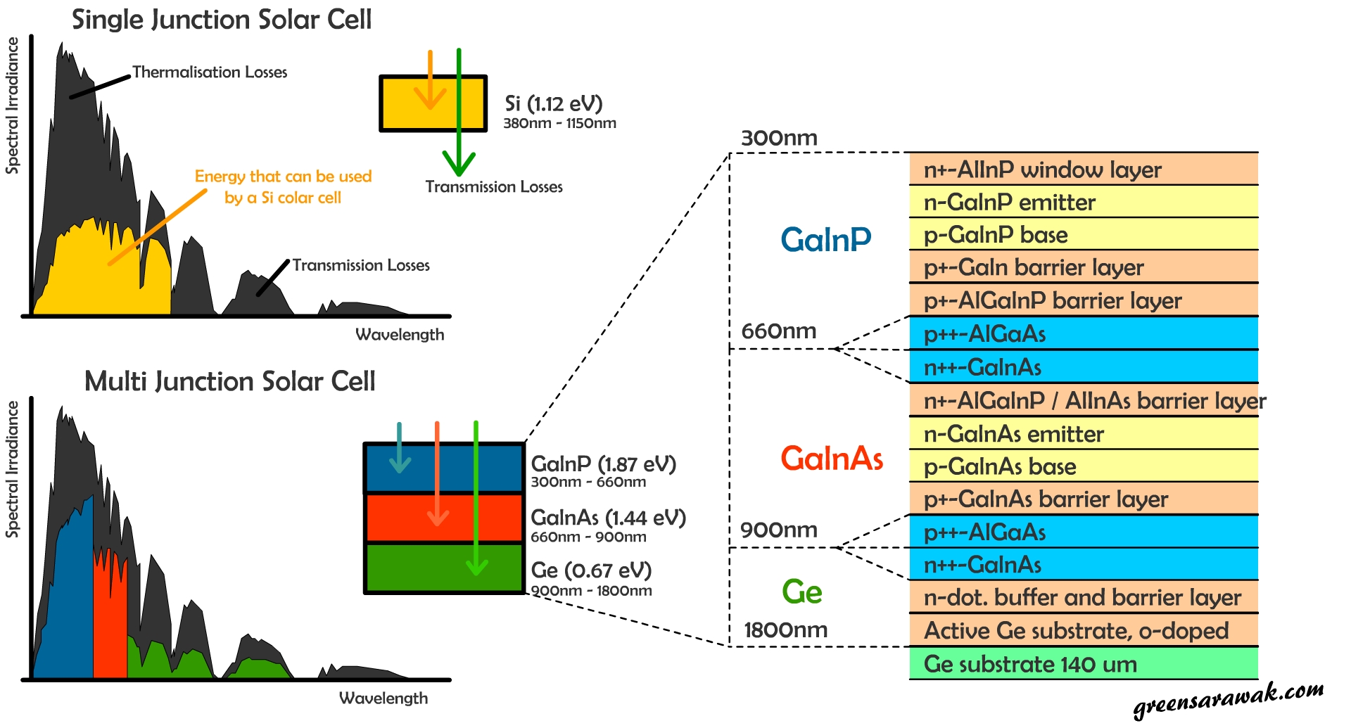
Showing how the two cells perform in converting the full spectrum of sunlight into electricity. In single junction silicon solar cell can accept photon with energy level more than 1.12eV, any energy more than 1.12eV is wasted as heat. In multi junction solar cell, different semiconductor can harvest photon of different energy level, hence increase the total efficiency.
Concentrated photovoltaic with multi junction solar cells had reach a solar cell efficiency of more than 44 per cent. However due to cost and complexity, it is still out of reach for normal consumer market.
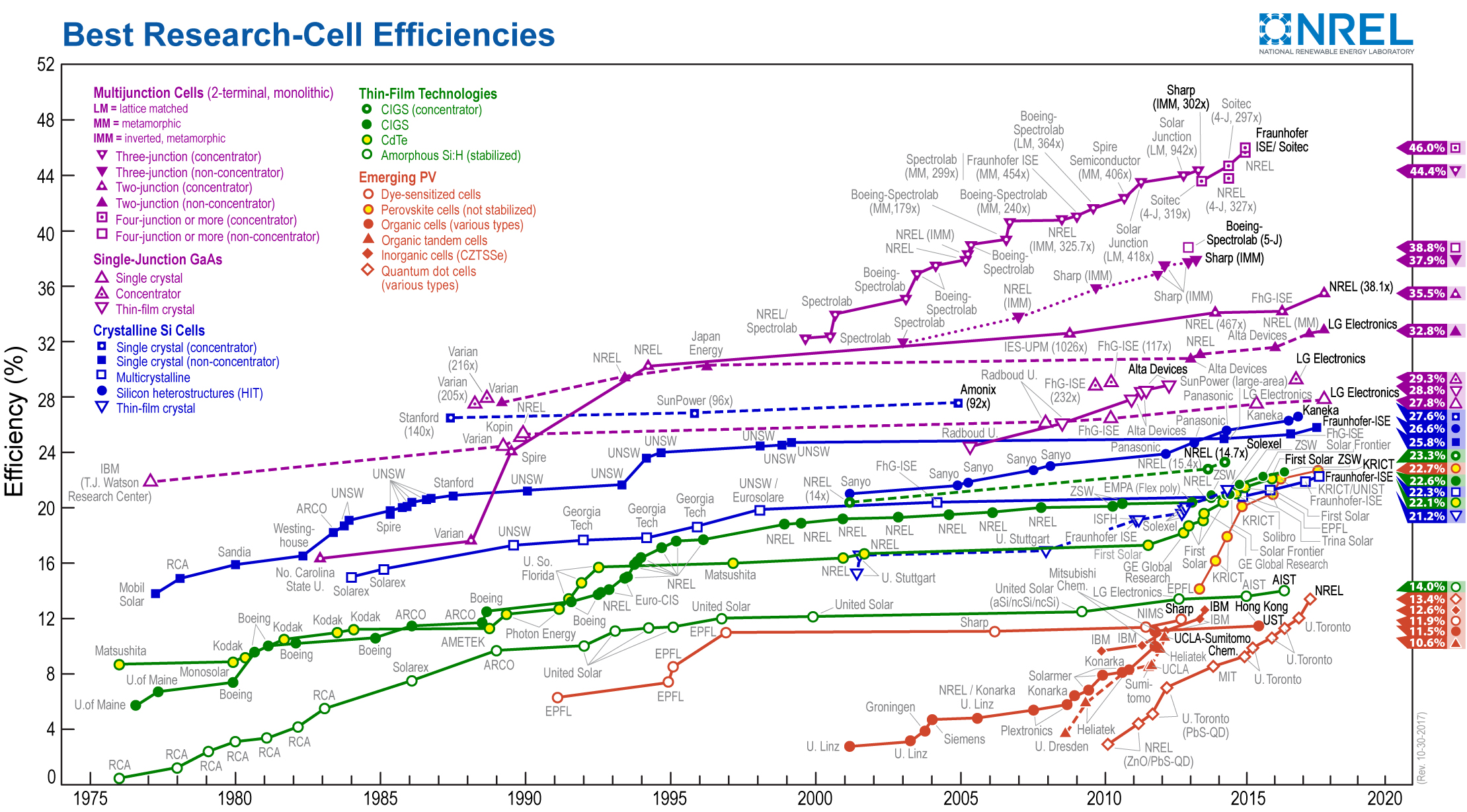
Source: National Renewable Energy Laboratory (NREL), Golden, CO
After we understand that monocrystalline is better efficiency than polycrystalline and thin film, does that means lets go and all buy mono crystalline panels and forget the rest ? The answer is no.
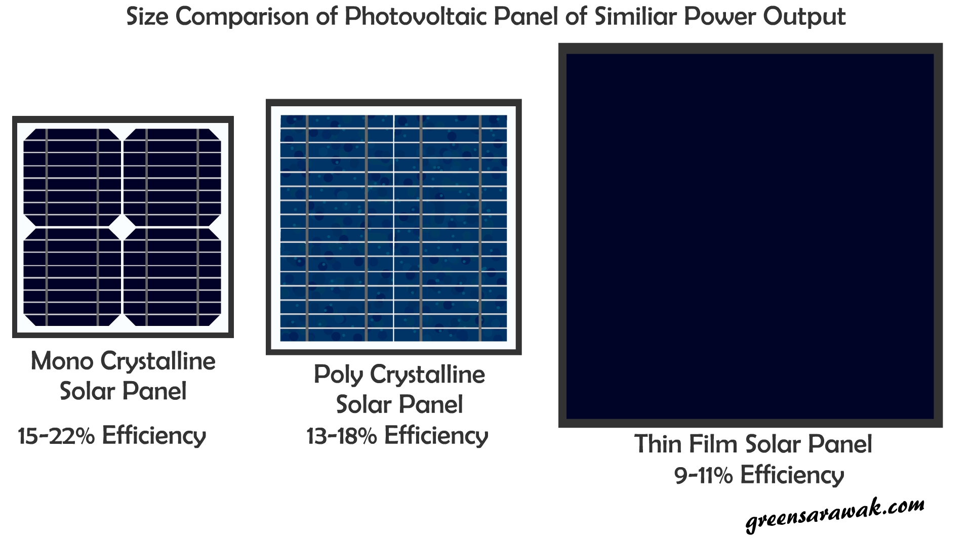
A 100watt rated poly crystalline panel produced the nearly the same amount of power output in comparison to a 100watt rated mono crystalline panel, but the poly crystalline panel will be bigger in surface compared to the mono crystalline panel to output the same amount of power. Thin film panel will be even bigger in surface to gain the same power output (depends on the photovoltaic materials used).
The decision on which panel to choose will depends on where are we putting the panels. In a small house with a small roof, it will wise to get a very high efficiency solar panel to get the most out of it. Obviously it come with a higher price tag. However if you have a whole grass land to spare for your solar project, you can easily get the same output with very cheap very low efficiency solar panel, but a coverage of more areas.